- 您现在的位置:买卖IC网 > Sheet目录329 > IDT70V9359L7BFI (IDT, Integrated Device Technology Inc)IC SRAM 144KBIT 7NS 100FBGA
IDT70V9359/49L
High-Speed 3.3V 8/4K x 18 Dual-Port Synchronous Pipelined Static RAM
Industrial and Commercial Temperature Ranges
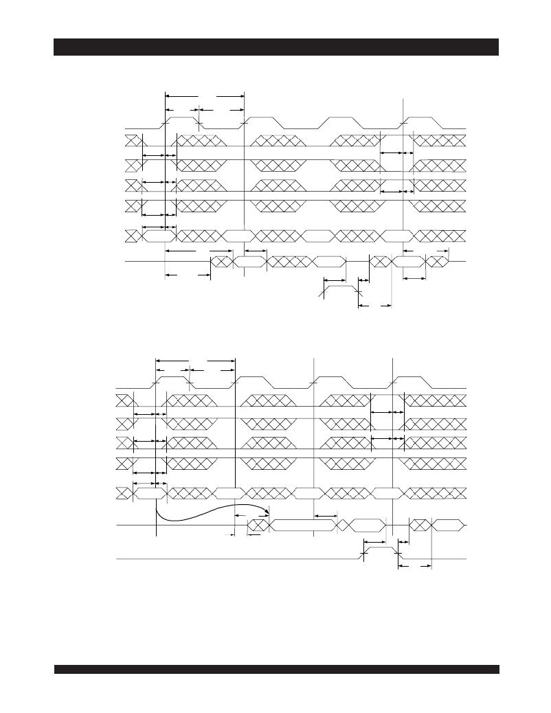
Timing Waveform of Read Cycle for Flow-Through Output
( FT /PIPE "X" = V IL ) (3,7)
t CYC1
CLK
CE 0
t CH1
t CL1
t SC
t HC
t SC
t HC
CE 1
t SB
t HB
UB , LB
R/ W
t SW t HW
t SA
t HA
t SB
t HB
ADDRESS
(5)
An
t CD1
An + 1
t DC
An + 2
An + 3
t CKHZ (1)
DATA OUT
Qn
Qn + 1
Qn + 2
t CKLZ
(1)
(1)
t OHZ
t OLZ
(1)
t DC
OE
(2)
t OE
Timing Waveform of Read Cycle for Pipelined Operation
( FT /PIPE "X" = V IH ) (3,7)
t CYC2
5638 drw 07
CLK
CE 0
t CH2
t CL2
t SC
t HC
t SC
t HC
(4)
CE 1
UB , LB
R/ W
t SB
t SW
t HB
t HW
t SB
(6)
t HB
t SA
t HA
(5)
ADDRESS
An
(1 Latency)
An + 1
t CD2
An + 2
t DC
An + 3
DATA OUT
Qn
Qn + 1
Qn + 2
(6)
t CKLZ
(1)
t OHZ
(1)
t OLZ
(1)
OE
(2)
t OE
NOTES:
1. Transition is measured 0mV from Low or High-impedance voltage with the Output Test Load (Figure 2).
2. OE is asynchronously controlled; all other inputs are synchronous to the rising clock edge.
3. ADS = V IL and CNTRST = V IH .
5638 drw 08
4. The output is disabled (High-Impedance state) by CE 0 = V IH , CE 1 = V IL
following the next rising edge of the clock. Refer to Truth Table 1.
5. Addresses do not have to be accessed sequentially since ADS = V IL constantly loads the address on the rising edge of the CLK; numbers
are for reference use only.
6. If UB or LB was HIGH, then the Upper Byte and/or Lower Byte of DATA OUT for Qn + 2 would be disabled (High-Impedance state).
7. "X' here denotes Left or Right port. The diagram is with respect to that port.
9
6.42
发布紧急采购,3分钟左右您将得到回复。
相关PDF资料
IDT70V9369L7PFI
IC SRAM 288KBIT 7NS 100TQFP
IDT70V9389L6PRF
IC SRAM 1.125MBIT 6NS 128TQFP
IDT71016S20YGI
IC SRAM 1MBIT 20NS 44SOJ
IDT71024S25TYGI
IC SRAM 1MBIT 25NS 32SOJ
IDT71124S20YGI
IC SRAM 1MBIT 20NS 32SOJ
IDT71256L35Y/2996
IC SRAM 256KBIT 35NS 28SOJ
IDT71256SA25PZGI
IC SRAM 256KBIT 25NS 28TSOP
IDT71321LA20TFG
IC SRAM 16KBIT 20NS 64STQFP
相关代理商/技术参数
IDT70V9359L7PF
功能描述:IC SRAM 144KBIT 7NS 100TQFP RoHS:否 类别:集成电路 (IC) >> 存储器 系列:- 标准包装:45 系列:- 格式 - 存储器:RAM 存储器类型:SRAM - 双端口,异步 存储容量:128K(8K x 16) 速度:15ns 接口:并联 电源电压:3 V ~ 3.6 V 工作温度:0°C ~ 70°C 封装/外壳:100-LQFP 供应商设备封装:100-TQFP(14x14) 包装:托盘 其它名称:70V25S15PF
IDT70V9359L7PF8
功能描述:IC SRAM 144KBIT 7NS 100TQFP RoHS:否 类别:集成电路 (IC) >> 存储器 系列:- 标准包装:45 系列:- 格式 - 存储器:RAM 存储器类型:SRAM - 双端口,异步 存储容量:128K(8K x 16) 速度:15ns 接口:并联 电源电压:3 V ~ 3.6 V 工作温度:0°C ~ 70°C 封装/外壳:100-LQFP 供应商设备封装:100-TQFP(14x14) 包装:托盘 其它名称:70V25S15PF
IDT70V9359L7PFI
功能描述:IC SRAM 144KBIT 7NS 100TQFP RoHS:否 类别:集成电路 (IC) >> 存储器 系列:- 标准包装:1,000 系列:- 格式 - 存储器:RAM 存储器类型:SRAM - 双端口,同步 存储容量:1.125M(32K x 36) 速度:5ns 接口:并联 电源电压:3.15 V ~ 3.45 V 工作温度:-40°C ~ 85°C 封装/外壳:256-LBGA 供应商设备封装:256-CABGA(17x17) 包装:带卷 (TR) 其它名称:70V3579S5BCI8
IDT70V9359L7PFI8
功能描述:IC SRAM 144KBIT 7NS 100TQFP RoHS:否 类别:集成电路 (IC) >> 存储器 系列:- 标准包装:45 系列:- 格式 - 存储器:RAM 存储器类型:SRAM - 双端口,异步 存储容量:128K(8K x 16) 速度:15ns 接口:并联 电源电压:3 V ~ 3.6 V 工作温度:0°C ~ 70°C 封装/外壳:100-LQFP 供应商设备封装:100-TQFP(14x14) 包装:托盘 其它名称:70V25S15PF
IDT70V9359L9BF
功能描述:IC SRAM 144KBIT 9NS 100FBGA RoHS:否 类别:集成电路 (IC) >> 存储器 系列:- 标准包装:45 系列:- 格式 - 存储器:RAM 存储器类型:SRAM - 双端口,异步 存储容量:128K(8K x 16) 速度:15ns 接口:并联 电源电压:3 V ~ 3.6 V 工作温度:0°C ~ 70°C 封装/外壳:100-LQFP 供应商设备封装:100-TQFP(14x14) 包装:托盘 其它名称:70V25S15PF
IDT70V9359L9PF
功能描述:IC SRAM 144KBIT 9NS 100TQFP RoHS:否 类别:集成电路 (IC) >> 存储器 系列:- 标准包装:45 系列:- 格式 - 存储器:RAM 存储器类型:SRAM - 双端口,异步 存储容量:128K(8K x 16) 速度:15ns 接口:并联 电源电压:3 V ~ 3.6 V 工作温度:0°C ~ 70°C 封装/外壳:100-LQFP 供应商设备封装:100-TQFP(14x14) 包装:托盘 其它名称:70V25S15PF
IDT70V9359L9PF8
功能描述:IC SRAM 144KBIT 9NS 100TQFP RoHS:否 类别:集成电路 (IC) >> 存储器 系列:- 标准包装:72 系列:- 格式 - 存储器:RAM 存储器类型:SRAM - 同步 存储容量:9M(256K x 36) 速度:75ns 接口:并联 电源电压:3.135 V ~ 3.465 V 工作温度:-40°C ~ 85°C 封装/外壳:100-LQFP 供应商设备封装:100-TQFP(14x14) 包装:托盘 其它名称:71V67703S75PFGI
IDT70V9369L12PF
功能描述:IC SRAM 288KBIT 12NS 100TQFP RoHS:否 类别:集成电路 (IC) >> 存储器 系列:- 标准包装:45 系列:- 格式 - 存储器:RAM 存储器类型:SRAM - 双端口,异步 存储容量:128K(8K x 16) 速度:15ns 接口:并联 电源电压:3 V ~ 3.6 V 工作温度:0°C ~ 70°C 封装/外壳:100-LQFP 供应商设备封装:100-TQFP(14x14) 包装:托盘 其它名称:70V25S15PF